3D-Micromac Signs MOU with dpiX to Formalize Partnership for Flat Panel Sensor Manufacturing
dpiX and 3D-Micromac America today announced the signing of a Memorandum of Understanding (MOU) that outlines the companies’ cooperation in the development, prototyping and manufacturing of laser-manufactured flat panel sensor semiconductors.
dpiX and 3D-Micromac America envision that the partnership will enhance the value chains for the U.S.-based, multi-segment semiconductor foundry operated by dpiX and the semiconductor and display segments of 3D-Micromac America’s business.“For over 20 years, we have been and continue to be the worldwide market leader in flat panel optical sensors for radiology. With great pride, we now see that our foundry services are also rapidly attracting strategic partners in R&D, prototyping and manufacturing for different types of flat panel semiconductors” said Frank Caris, CEO and president of dpiX.
dpiX and 3D-Micromac share the belief that their combined strengths – a U.S.-based semiconductor facility, industry-leading research and development (R&D), product development and end-product manufacturing capabilities – will contribute to the United States retaining and expanding upon these unique value chains to meet U.S. demand and compete internationally. Seeing these goals to fruition, however, requires appropriate funding. Both companies are monitoring progress of the CHIPS for America Act, the Biden-Infrastructure Plan and the Strategic Competition Act, with great anticipation.
“Partnering with dpiX means contributing precision laser expertise to a worthy endeavor. We look forward to adding a new dimension to the team and enhancing overall U.S. competitiveness in the sensor, display and electronics arena,” said Brian Hoekstra, president of 3D-Micromac America.
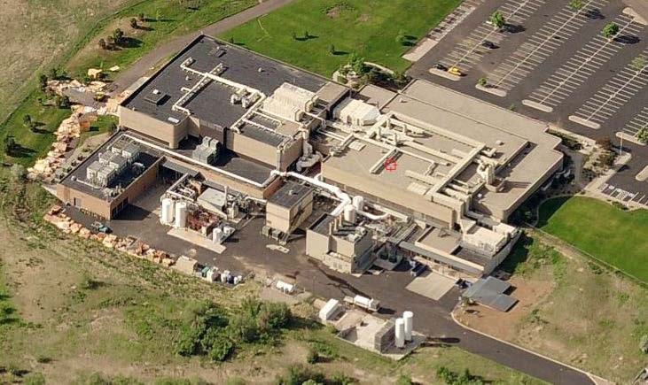
Headquartered in Colorado Springs, Colorado, dpiX is home to the largest A-Si Semiconductor production facility outside of Asia (150,000 square foot).
About dpiX
dpiX was established in 1999 in Silicon Valley, Calif., with the support of the United States Department of Defense and private investors. From its current headquarters in Colorado Springs, Colo., where the company invested over $250M in a trusted and IP-secure semiconductor production facility (the largest A-Si semiconductor cleanroom facility outside of Asia), dpiX provides the foundation for some of today’s most innovative solutions in medical, industrial, military and security imaging. dpiX is the market leader in state-of-the-art optical semiconductors for radiology (A-Si). Although dpiX is a small company, it remains at the forefront of the semiconductor industry through strategic partnerships with a wide range of partners in research, design, prototyping and more. Current shareholders include Siemens Healthineers, Philips, Thales and Varex. Learn more at https://www.dpix.com.
Contact:
dipX
Celeste Lucero
celeste.lucero@dpix.com
719-332-0570
About 3D-Micromac
Founded in 2002, 3D-Micromac AG is the industry leader in laser micromachining, delivering powerful, user-friendly and leading-edge processes with superior production efficiency. We develop processes, machines and turnkey solutions at the highest technical and technological level. 3D-Micromac systems and services have been successfully implemented in various high-tech industries worldwide, including photovoltaic, semiconductor, glass and display industries, micro diagnostics, and medical technology.


