3D-Micromac to present breakthroughs in laser micromachining for semiconductor manufacturing and advanced packaging at SEMICON West
Power devices, magnetic sensors, microLEDs, and advanced packaging among myriad applications enabled by 3D-Micromac’s laser micromachining solutions
Chemnitz, Germany, July 5, 2023—3D-Micromac AG, the industry leader in laser micromachining and roll-to-roll laser systems for the semiconductor, photovoltaic, glass and display markets, today announced that new developments with its laser micromachining solutions used in manufacturing power devices, magnetic sensors, and microLEDs, as well as in semiconductor advanced packaging, will be highlighted at SEMICON West, to be held July 11-13, 2023 in San Francisco.
“Since the first working laser was developed more than 60 years ago, lasers have been used in a wide array of industrial markets. Within the semiconductor industry, lasers play many roles, from wafer dicing, surface structuring, and sample preparation to ablation, sintering, via drilling and patterning. As the leading specialist in laser micromachining, 3D-Micromac offers cost-effective, scalable and versatile products and solutions to support our customers’ needs from development and prototyping through volume production. We look forward to highlighting these solutions, as well as the many applications that they enable, next week at SEMICON West,” stated Uwe Wagner, CEO of 3D-Micromac.
Laser annealing improves power device performance
According to Yole Intelligence, the silicon carbide (SiC) power device market is projected to achieve a compound annual growth rate (2021-2027) of more than 30 percent to reach beyond US$6 billion in 2027(1). Benefits of SiC power devices include boosting power efficiency and minimizing energy loss in electric vehicles (EVs), hybrid EVs, power supplies, and solar and wind inverters. While much goes into the development of SiC power devices, the formation of ohmic contacts on the backside of these devices plays a key role in defining their electrical characteristics and mechanical strength.
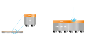
The microPRO™ XS OCF system from 3D-Micromac is ideally suited for ohmic contact formation (OCF) in SiC power devices due to its high precision and repeatability, and low thermal leakage, which prevent thermal damage to the wafer frontside that can negatively affect device performance. The system features a UV-wavelength diode-pumped solid-state laser source with nano-second pulses and spot scanning to process the entire metalized backside of SiC wafers while preventing the generation of large carbon clusters and heat-related damage to the frontside of the wafer. New features include:
- Large energy density process window that ensures constant stable forward voltage, leading to higher uptime and yield
- Special tool design that minimizes footprint and lowers cost of ownership
- Ability to process 200-mm SiC wafers without stitching, which avoids the creation of dead zones that can negatively impact yield and device quality
The microPRO™ XS OCF system from 3D-Micromac is ideally suited for ohmic contact formation in SiC power devices due to its high precision and repeatability, and low thermal leakage, which prevent thermal damage to the wafer frontside that can negatively affect device performance.
Laser annealing for high-volume magnetic sensor production
Growth in the magnetic sensor market is being driven by position, speed and angle sensing needs across consumer and industrial applications, including automobiles, smartphones, wearables and robotics. Thermal annealing has traditionally been used to maximize the magnetoresistance effects of magnetic sensors. However, this approach requires multiple steps to produce sensors with different magnetic orientations that are then mounted in multi-chip packages or processed as integrated monolithic packages. This adds significantly to production costs and cycle time.
The microVEGA® xMR system from 3D-Micromac provides high-throughput laser annealing for monolithic magnetic sensor formation. A highly flexible tool, the microVEGA xMR can accommodate both Giant Magnetoresistance (GMR) and Tunnel Magnetoresistance (TMR) sensors, as well as easily adjust magnetic orientation, sensor position and sensor dimension. This makes it an ideal solution for magnetic sensor production. The system provides extremely high throughput of up to 500,000 sensors per hour with the current-generation platform. New developments on the horizon including a new beam positioning system will enable even greater throughput rates.
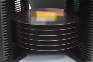
Tunnel Magnetoresistance (TMR) sensor wafers processed with the microVEGA® xMR selective laser annealing system from 3D-Micromac.
Laser-based sample preparation accelerates microstructure diagnostics and FA
Cutting and preparing samples from semiconductor wafers, dies and packages for microstructure diagnostics and failure analysis (FA) is an essential but time-consuming and costly step. Focused ion beam (FIB) micromachining can take several hours to prepare a typical sample. In addition, FIB only allows for very small sample sizes, and wastes precious FIB time by “digging” excavations needed for cross-sectional imaging. Reaching larger depths or widths is severely restricted by the limited ablation rate.
The microPREP™ PRO system from 3D-Micromac enables laser-based sample preparation for a variety of specimen preparation applications. It complements existing approaches to sample preparation by off-loading the vast majority of sample prep work from the FIB tool and relegating FIB to final polishing. As a result, the microPREP PRO significantly reduces time to final sample to less than one hour in many cases.
New semiconductor applications for the microPREP PRO include preparing chunks and wedding cake structures for micro/nano X-ray tomography, cross sections, delayering, decapping, and ablation of layers to expose wires for probing and testing. The microPREP PRO also supports microLED manufacturing by enabling lift-out of defective microLEDs for subsequent inspection and failure analysis.
3D-Micromac also recently introduced its new microPREP PRO FEMTO system, which features a femtosecond laser source and optimized optical setup to provide high-speed atom probe tomography (APT). The microPREP PRO FEMTO reduces APT sample prep time from hours to minutes with millimeter-precision while avoiding thermal damage to the sample.
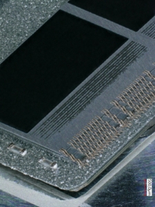
Sample preparation of a chip using the microPREP PRO from 3D-Micromac to access to the wires for subsequent failure analysis (FA). The laser is used to remove the cover and gain access to the single features. The microPREP PRO can also be used to cut these connections to run additional FA tests on devices.
See 3D-Micromac at SEMICON West
SEMICON West attendees interested in learning more about 3D-Micromac and its suite of laser micromachining solutions are invited to visit 3D-Micromac at the Moscone Center South Hall, Booth 1064 on July 11-13 in San Francisco.
References
(1) Power SiC 2022 Report, Yole Intelligence, March 2022, https://www.yolegroup.com/product/report/power-sic-2022/
About 3D-Micromac
Founded in 2002, 3D-Micromac AG is the industry leader in laser micromachining, delivering powerful, user-friendly and leading-edge processes with superior production efficiency. We develop processes, machines and turnkey solutions at the highest technical and technological level. 3D-Micromac systems and services have been successfully implemented in various high-tech industries worldwide, including photovoltaic, semiconductor, glass and display industries, micro diagnostics, and medical technology.


