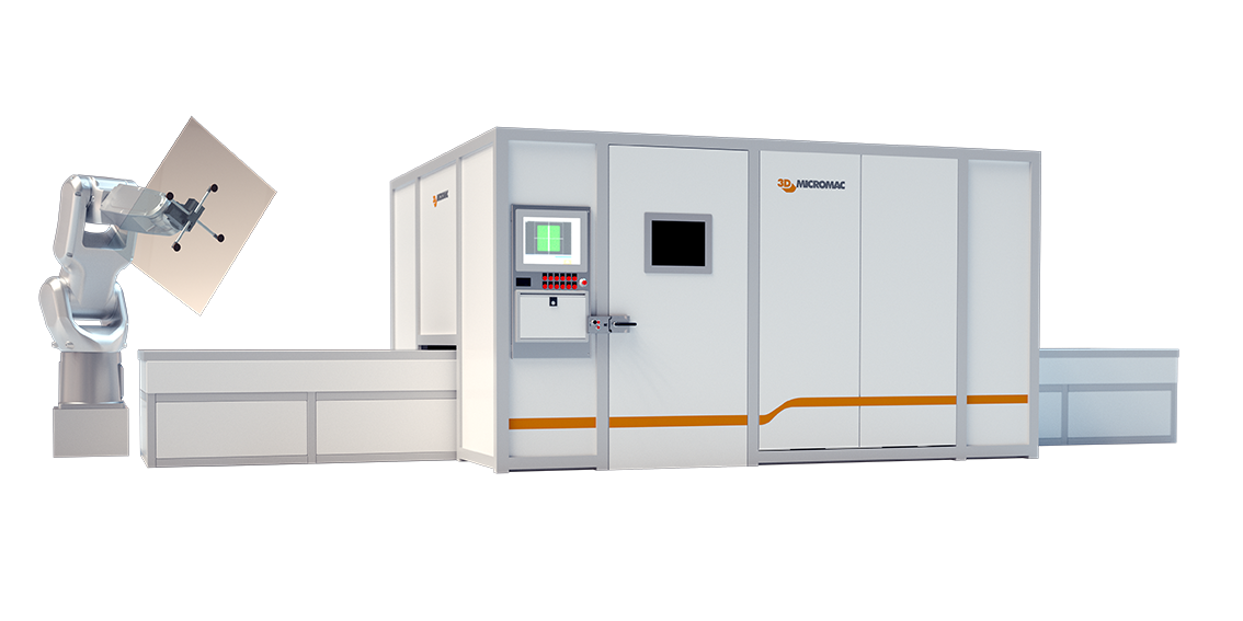
Laser Annealing

High-throughput laser annealing enables ohmic contact formation (OCF) of SiC power devices and magnetic processing of monolithic integrated sensors.

Power Device Applications

The silicon carbide (SiC) power device market is experiencing double-digit growth due to the benefits of SiC in boosting power efficiency and minimizing energy loss in applications such as automotive electric vehicles (EVs) and hybrid EVs, power supplies, and solar inverters.

The formation of ohmic contacts on the backside of SiC power devices plays a key role in defining the electrical characteristics and mechanical strength of the device. Traditionally, thermal annealing processes using flash lamps with millisecond pulses have been used for OCF on the backside of SiC wafers.

Because this process requires temperatures of upwards of 1000° C, which can be detrimental to structures on the front side of the wafers, flash lamps are limited to wafer thicknesses of 350 microns and above.

As the industry migrates to thinner SiC power devices for improved electrical performance and thermal management, new annealing solutions are needed to minimize these thermal effects. Laser annealing using UV nanosecond pulses with the help of our microPRO XS OCF provides the high precision and repeatability required for OCF on the backside of SiC wafers while ensuring no thermal damage to the wafer front side that can negatively affect device performance.

Magnetic Sensor Applications

The magnetic sensor device market is also experiencing strong growth driven by increased demand for magnetic sensors in consumer electronics such as rotation sensors and e-compasses in smartphones and wearables, in appliances such as linear position sensors and angle sensors for brushless DC motors, and in automotive applications such as power steering angle detection and electronic throttle control.

Thermal annealing has traditionally been used to maximize the magnetoresistance effects of Giant Magnetoresistance (GMR) and Tunneling Magnetoresistance (TMR) sensors. However, this approach requires multiple process steps to produce sensors with different magnetic orientations mounted in multi-chip packages or processed as integrated monolithic packages.

Selective laser annealing using our microVEGA xMR provides several advantages over thermal annealing for magnetic sensor manufacturing. These include higher precision to enable the processing of smaller magnetic device structures, more devices per wafer, and the ability to set different reference magnetization directions on sensors across a single wafer—reducing process steps, simplifying the overall production flow, and enabling more cost-effective production of integrated monolithic sensor packages.

Contact

Please contact our technical sales team for more information.

Frank Richter
Tel: +49 371 40043-222
sales@3d-micromac.com

OCF Process

xMR Sensor Formation

microVEGA xMR-Process Video

Keep up with our Newsletter!

Receive early access to our webinars, whitepapers and case studies.

Don’t miss any events, special offers or updates to our products.

Recommended Laser System